Tiger Lake VMD Controller question

IntelgEEk

Member
I have a HP Pavilion X360 14m-dw1023dx laptop with a Core i5-1135G7 CPU.

According to HWiNFO64, this CPU has a RST VMD Controller with a PCIe 2.0 bus (see attachments) which is connected to a Samsung MZVLQ256HAJD-000H1 PCIe 3.0 x4 NVMe M.2 SSD.

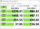
Since PCIe 2.0 x4 is limited to 2.0 GB/s, how is it possible that the SEQ1M Q8T1 sequential read speed reported by CrystalDiskMark exceeds 2.2 GB/s?

This CrystalDiskMark result is theoretically impossible from a PCIe 2.0 x4 bus, but is easily achievable from a PCIe 3.0 x4 bus.

Is HWiNFO64 reporting erroneous information about the actual PCIe bus used by the RST VMD controller?
 

Attachments

This might be possible if the link width/speed would dynamically change depending on activity which is quite common for some devices.
The main window of HWiNFO doesn't refresh information in real-time, so you might try to start HWiNFO new when the drive is active (running a benchmark).
 
This might be possible if the link width/speed would dynamically change depending on activity which is quite common for some devices.
The main window of HWiNFO doesn't refresh information in real-time, so you might try to start HWiNFO new when the drive is active (running a benchmark).
According to my 1st HWiNFO64 attachment, the current link width is "Not negotiated."
Note that PCIe 2.0 x8 would support 2.2 GB/s sequential reads, but all PCIe 3.0 NVMe M.2 SSDs only support x4; PCIe 3.0 NVMe M.2 SSDs do not support x8.
 
I tried your suggestion about starting HWiNFO64 during a CrystalDiskMark benchmark test, but nothing changed on the VMD controller screen (I even started HWiNFO64 several times during the benchmark test). It's rather curious why Intel is using the VMD controller on 11th gen laptops instead of the OEM (Samsung) NVMe controller. Seems like the VMD controller is more suited to desktops with RAID.
 
However, it's entirely possible that the VMD controller is dynamically changing speed from PCIe 2.0 x4 to PCIe 3.0 x4.
 
The VMD controller is an internal part of the CPU/PCIe Root Complex.
What controller/device is shown under the drive node? Is it perhaps the VMD PCIe Complicance device ?
 
FYI; I am a retired Sr. Electronics Design Engineer.

Here is my limited understanding about the VMD controller which was copied from a HP white paper entitled "Intel Virtual RAID on CPU (VROC) For NVM Express (NVMe) SSD RAID":

• Each VMD controller supports four PCIe x4 NVMe SSDs.
• Each CPU PCIe x16 slot consumes one VMD controller.
• Each CPU PCIe x8 slot consumes one half of a VMD controller that is shared with other slots.
• Each CPU PCIe x4 slot consumes one fourth of a VMD controller that is shared with other slots.

I tried to attach this white paper, but it exceeded the server size limit.
I have attached (2) HWiNFO64 screen shots of 1) the VMD PCIe Compliance Function and 2) a screen shot of the NVMe drives info which shows the host controller is a VMD NVMe RAID.
I also have limited knowledge about the VMD PCIe Compliance Function. I hope this answers your questions.
 

Attachments

HWiNFO reports values from PCIe capability registers for each device so it shows only what the device says.
The VMD controller reports rather strange values as it doesn't report any link width parameters nor current link speed. So it looks like this information is not properly implemented in the device (perhaps intentionally).
 
Since the in-depth details about Intel's VMD controller are proprietary, I wouldn't be surprised if Intel is intentionally omitting info.

However, here is some additional info I just discovered from the Intel VROC (VMD NVMe RAID) Quick Configuration Guide, section 3, VMD:

"Each member of the Intel® Xeon® processor Scalable family has three Intel® VMD domains (numbered one,
two, and three). Each Intel® VMD domain manages 16 PCIe* lanes divided into four Intel® VMD ports (named
A, B, C, and D) consisting of four PCIe* lanes each. Some of these Intel® VMD ports are routed to specific
risers and slots in the system, while other Intel® VMD ports are routed to specific chipset uplinks, SAS
modules, or onboard Oculink connectors. This routing is fixed (non-configurable); please refer to the relevant
motherboard's Technical Product Specification for details on this routing.

Note: Intel® VMD ports routed to specific chipset uplinks cannot be used for Intel® VROC (VMD NVMe RAID)
configurations.

There are two different ways to connect NVMe* drives to Intel® VMD ports:
1. NVMe* drives connect directly to VMD ports in a 1:1 fashion when using the onboard Oculink* ports
or by using PCIe* retimers. Each NVMe* drive then uses four dedicated PCIe* lanes, providing full
bandwidth to each drive.
2. Several NVMe* drives connect to one VMD port by using either 8x4 or 8x8 PCIe* switches. Eight PCIe*
lanes are then shared by the NVMe* ports, providing limited bandwidth to each drive."

For whatever reason, Intel is also using their VMD controller on 11th gen Tiger Lake laptops.
Based on the CrystalDiskMark sequential read results, the only logical conclusion I can reach is that the VMD controller is dynamically changing speed from PCIe 2.0 x4 to PCIe 3.0 x4.
 
My interpretation of all this stuff is each NVMe drive connected to a VMD port is provided full bandwidth from the PCIe bus.
So in the case of my Tiger Lake laptop, the Samsung PCIe 3.0 x4 NVMe M.2 SSD is effectively connected to a PCIe 3.0 x4 bus.
 
This makes perfect sense since manufacturers shouldn't have to provide separate PCIe 2.0, 3.0, and 4.0 buses in laptops like they do for desktops. You can think of each VMD port like a fire hydrant, which is a brilliant idea from Intel.
 
Here's a better technical explanation about the VMD:

Effectively, the Intel VMD enables virtual HBAs (Host Bus Adapters) for the connected NVMe SSDs, which allows the SSDs to have direct access to the CPU, removing the need for an HBA entirely.
 
Back
Top