And who told you that the CPU -Z shows the right meanings?
")
It shows more or less - the correct numbers only when the stars are converged, in other cases it removes the nonsense of the blue mare.
For example, it is lying when reading the SPD Modules of the RAM. I have in my cars, the RE ECC DDR3-1866M (PC3-14900R -2-12-E2) is worth it, but the CPU-Z reads 888 MHz from the SPD and says that this is PC3-14200, although the CPUID was reported about this bug at the end 2010, but the company recognized its presence a few years after the public scandal and promising to fix it has not done this so far.
In the same way, in her “benchmark”, a slow reference processor often turns out to be much faster than the tested, in their website there are delusional in principle not achievable “dispersal records”: for example, the maximum multiplier is 42, but the processor operates at a frequency of about 9 GHz at 102 MHz according to 102 MHz at FSB, but CPUID confirms this.
This utility is not able to distinguish twelve-core's Xeon E5 2000 from the six-core's Core i7-3000X, and server C602 chipset from desktop X79-for it this is the same thing, and the C600th series chipsets do not exist at all.
Also, for visual compare:
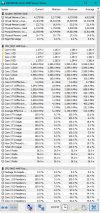
Read SPD for Samsung M393B2G70QH0-CMA
CPU-Z v2.05.1 x64 (13.03.2023)
Detect as PC3-14200 (889 MHz)
JEDEC timings tableCL-tRCD-tRP-tRAS-tRC @ frequency
JEDEC #1 6.0-6-6-16-22 @ 457 MHz
JEDEC #2 7.0-7-7-19-26 @ 533 MHz
JEDEC #3 8.0-8-8-21-29 @ 609 MHz
JEDEC #4 9.0-9-9-24-33 @ 685 MHz
JEDEC #5 10.0-10-10-26-36 @ 761 MHz
JEDEC #6 11.0-11-11-29-40 @ 838 MHz
JEDEC #7 13.0-12-12-31-42 @ 888 MHz
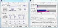
HWiNFO64 7.41-5010
JEDEC timings tableCL-tRCD-tRP-tRAS-tRC @ frequency
Detect as PC3-14900 (933,7 MHz)
JEDEC #1 6-6-6-14 @400.0 MHz
JEDEC #2 7-7-7-19 @533.3 MHz
JEDEC #3 9-9-9-23 @666.7 MHz
JEDEC #4 11-11-11-28 @800.0 MHz
JEDEC #5 13-13-13-32 @933.3 MHz
Notes - all string is exists in to SPD
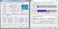
Thaiphoon Burner Super Blaster
Manufacturing Description
Module Manufacturer: Samsung
Module Part Number: M393B2G70QH0-CMA
DRAM Manufacturer: Samsung
DRAM Components: K4B4G0446Q-HCMA
DRAM Die Revision / Process Node: Q / Not determined
Register Manufacturer: IDT
Register Model: A1 (Evergreen)
Module Manufacturing Date: Week 48, 2014
Manufacturing Date Decoded: November 24-28, 2014
Module Manufacturing Location: Suzhou, China (SESS)
Module Serial Number: xxxxxxxxh
Lot Number: xxxxxxx
Module Revision: 0000h
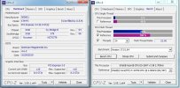
Physical & Logical Attributes
Fundamental Memory Class: DDR3 SDRAM
Module Speed Grade: DDR3-1866M
Module Type: RDIMM (133,35 mm)
Module Capacity: 16 GB
Reference Raw Card: E2 (10 layers)
JEDEC Raw Card Designer: Not determined
Module Nominal Height: 29 < H <= 30 mm
Module Thickness Maximum, Front: 1 < T <= 2 mm
Module Thickness Maximum, Back: 1 < T <= 2 mm
Number of Registers on RDIMM: 1
Number of Rows of DRAMs on RDIMM: 2
Number of DIMM Ranks: 2
Address Mapping from Edge Connector to DRAM: Mirrored
DRAM Device Package: Standard Monolithic
DRAM Device Package Type: 78-ball FBGA
DRAM Device Die Count: Not specified
Signal Loading: Not specified
Number of Column Addresses: 11 bits
Number of Row Addresses: 16 bits
Number of Bank Addresses: 3 bits (8 banks)
DRAM Device Width: 4 bits
Programmed DRAM Density: 4 Gb
Calculated DRAM Density: 4 Gb
Number of DRAM components: 36
DRAM Page Size: 1 KB
Primary Memory Bus Width: 64 bits
Memory Bus Width Extension: 8 bits
Supported Voltage Levels: 1.50 V
DRAM Timing Parameters
Fine Timebase Dividend: 1
Fine Timebase Divisor: 1
Fine Timebase: 0,0010 ns
Medium Timebase Dividend: 1
Medium Timebase Divisor: 8
Medium Timebase: 0,125 ns
CAS# Latencies Supported (tCL): 6T, 7T, 8T, 9T, 10T,
11T, 13T
Minimum Clock Cycle Time (tCK min): 1,071 ns (933,71 MHz)
CAS# Latency Time (tAA min): 13,125 ns
RAS# to CAS# Delay Time (tRCD min): 13,125 ns
Row Active to Row Active Delay (tRRD min): 5,000 ns
Row Precharge Delay Time (tRP min): 13,125 ns
Active to Precharge Delay Time (tRAS min): 34,000 ns
Act to Act/Refresh Delay Time (tRC min): 47,125 ns
Refresh Recovery Delay Time (tRFC min): 260,000 ns
Write Recovery Time (tWR min): 15,000 ns
Write to Read Command Delay (tWTR min): 7,500 ns
Read to Precharge Command Delay (tRTP min): 7,500 ns
Four Active Windows Delay (tFAW min): 27,000 ns
RZQ / 6 Drive Strength: Supported
RZQ / 7 Drive Strength: Supported
DLL-Off Mode Support: Supported
Thermal Parameters
Extended Temperature Range: 0-95 °C
Extended Temperature Refresh Rate: 2X (85-95 °C)
Auto Self Refresh (depending on temperature): Not supported
Module Thermal Sensor: Incorporated
On-die Thermal Sensor Readout: Not supported
Partial Array Self Refresh: Not supported
Heat Spreader Solution: Not Incorporated
Integrated Temperature Sensor
Manufacturer: Microchip
Model: MCP98243
Revision: 01h
Temperature Monitor Status: Active
Current Ambient Temperature: 43,750 °C
Sensor Resolution: 0,2500 °C (10-bit ADC)
Accuracy over the active range (75 °C to 95 °C): ±1 °C
Accuracy over the monitoring range (40 °C to 125 °C): ±2 °C
Open-drain Event Output: Disabled
10V of VHV on A0 pin: Supported
Negative Temperature Measurements: Supported
Interrupt capabilities: Supported
SMBus timeout period for TS access: 25 to 35 ms
SPD Protocol
SPD Revision: 1.2
SPD Bytes Total: 256
SPD Bytes Used: 176
SPD Checksum: F03Ch (OK)
CRC covers bytes: 0-116
Part number details
JEDEC DIMM Label: 16GB 2Rx4 PC3-14900R-12-12-E2
Classification: DDR3 SDRAM (1.5V VDD)
Module Type: 240-pin Registered DIMM
Module Speed: DDR3-1866 13-13-13
Module Revision: Mother PCB
Component Density: 8 Banks, SSTL(1.5V)
Component Configuration: x4
Memory Depth: 2G
Data Width: 72-bit
Die Generation: Q (3rd Gen)
Package Type: FBGA (Lead & Halogen Free)
AMB Vendor & Revision: N/A
Power Consumption: 0°C-85°C / Normal Power
Frequency CAS RCD RP RAS RC RFC RRD WR WTR RTP
933 MHz 13 13 13 32 44 243 5 14 7 7
800 MHz 11 11 11 28 38 208 4 12 6 6
667 MHz 10 9 9 23 32 174 4 10 5 5
667 MHz 9 9 9 23 32 174 4 10 5 5
533 MHz 8 7 7 19 26 139 3 8 4 4
533 MHz 7 7 7 19 26 139 3 8 4 4
400 MHz 6 6 6 14 19 104 2 6 3 3
From the series "
Find at least one coincidence."